OrCAD PCB Designer with Pspice
For proven, scalable, cost-effective PCB editing and routing
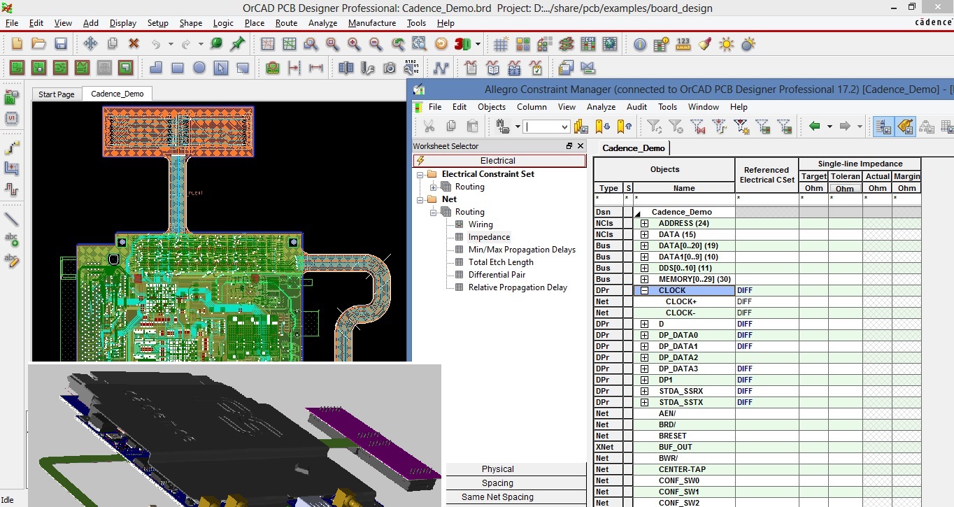
The Cadence® OrCAD® PCB Designer suite contains everything needed to take a PCB design from concept to production with a fully integrated design flow - including design capture, component tools, a PCB editor, and an auto/interactive router as well as interfaces for manufacturing, and mechanical CAD.
KEY TECHNOLOGIES
- Cadence OrCAD Capture, a comprehensive solution for entering, modifying, and verifying complex system designs quickly and cost-effectively
- Cadence OrCAD PCB Editor, based on Allegro technology: an intuitive, easy-to-use, constraint-driven environment for creating and editing simple to complex PCBs
- Cadence SPECCTRA® for OrCAD, the leading solution for automatic and interconnect PCB routing
- Cadence PSpice® A/D, a full-featured analog simulator with support for digital elements
BENEFITS
- Proven, scalable, cost-effective PCB editing and routing solution that grows as needed
- Provides a complete interconnect environment
- Includes a comprehensive feature set
- Features a front-to-back constraint management system for constraint creation, management, and validation
- Increases productivity through application integration
- Tight front-to-back integration
FEATURES
Design Capture Technology
OrCAD Capture offers a comprehensive solution for entering, modifying, and verifying complex system designs quickly and cost-effectively.
SCHEMATIC EDITING enables users to place and connect parts from a comprehensive set of functional libraries.
PROJECT MANAGEMENT enables users to collect and organize all the resources needed for the project throughout the design flow.
HIERARCHICAL DESIGN AND REUSE enables subcircuit reuseâ€"without having to make multiple copies.
LIBRARIES AND PART EDITING enables users to create and edit parts in the library or directly from the schematic page without interrupting workflow.
EASY DATA ENTRY allows designers to access all part, net, pin, and title block properties or any subset and make changes quickly through the spreadsheet property editor.
PCB Editor Technology
FEATURE SUMMARY
| Unlimited database | Exposed copper DRC |
| Netlist/crossplace/crossprobe | Interactive routing/etch editing |
| Padstack and symbol editor | Automatic silkscreen generation |
| Split plane support | Customizable/automated drill legend/NC output |
| Multiple via sizes, blind/buried via support | SKILL runtime, macro, and script support |
| Autoplacement/Quickplace/Floorplanner | Variant assembly drawing creation |
| IFF import | Variant bill-of-materials generation |
| 2-D drafting and dimensioning | Dynamic shapes with real-time plowing and healing |
| Gerber 274X, 274D artwork output generation | CAD interfaces â€" DXF (Ver.14), IDF (Ver. 2 and 3) |
| Multiple UNDO/REDO | PCB interfaces â€" OrCAD Layout, PADS (Ver.5), P-CAD (Ver.8) |
| Valor ODB++, ODB++(X) and universal viewer | Constraint manager (physical, spacing, properties, and DRC) |
| HTML-based reports | Manual testprep |
PCB EDITING ENVIRONMENT provides an intuitive, easy-to-use, constraint-driven environment for creating and editing simple to complex PCBs.
CONSTRAINT MANAGEMENT system displays physical and spacing rules along with a spreadsheet interface that enables the user to define, manage, and validate the different rules in a hierarchical fashion.
FLOORPLANNING AND PLACEMENT is driven by the constraint and rules-driven methodology.
INTERACTIVE ETCH EDITING delivers controlled automation to maintain user control, while maximizing routing productivity.

Dynamic push-and-shove capabilities make interactive editing easy
DYNAMIC SHAPES technology offers real-time copper pour plowing/healing functionality. Shape parameters can be applied at three different levels.
PCB MANUFACTURING features include a full suite of photo-tooling, bare-board fabrication and test outputs, including Gerber 274x, NC drill, and bare-board test, generated in a variety of formats.
PCB Autorouter Technology
FEATURE SUMMARY
| 6 signal layer limit | Interactive via search |
| Shape-based or gridded autorouting | Interactive routing with shoving and plowing |
| SMD fanout | Interactive Floorplanning |
| Trace width by net and net classes | Online design rule checking |
| Staggered pin support | Flip, rotate, align, push, and move components |
| 45-degree ECO routing | Placement density analysis |
| Memory pattern routing (SMD or through-hole) |
AUTOMATED INTERCONNECT ENVIRONMENT solves the challenges of complex interconnect routing with powerful, automated technology.
AUTOROUTING with fast, high completion rates. Routing algorithms are designed to handle a wide range of PCB interconnect challenges from simple to complex, low density to high density.
INTERACTIVE ROUTE EDITING simplifies and streamlines the etch editing process. As new conductors are routed, the plowing feature automatically pushes aside existing conductors and routes around pins.
PLACEMENT EDITING allows designers to quickly place components while simultaneously evaluating space, logic flow, and congestion before beginning the route or as needed during the routing process.
PCB EDITOR INTEGRATION Through the PCB editor interface, all design information and constraints are automatically passed to the router. Once the route is completed, all route information is automatically passed back to the PCB editor.
New features in Release 16.6
Placement Application Mode, Replication, Differential Pair, Constraint Region, Max Length, Interactive Etch Tuning, Automatic Test Pre, Via label, Associative Dimensioning, Cross Section Chart for Manufacture, Support of Stipple Patterns for the color, Color display of the nets in the constraint manager, Support for Dynamic Layer visibility in 3D Viewer, Pre- & Post-route signal integrity analysis, Graphical topology definition and exploration, Interactive waveform viewer, Macro modelling support (DML), IBIS5.0 support, IBISICM model support, Spectre-to-DML, HSPICE-to-IBIS, Lossy transmission lines, Coupled (3 net) simulation, Differential pair exploration and
Simulation
Optional Advanced Simulation Technology
PSpice A/D is a full-featured analog simulator with support for digital elements to help solve virtually any design challenge from high-frequency systems to low-- IC designs
--------------------------------------------------------------------------------------------------------------------------------------------------------------------------------------------------------
Click on Data Sheet to download
![]()
![]() OrCAD PCB Designer with Pspice Data Sheet
OrCAD PCB Designer with Pspice Data Sheet
Click on image for enlarged view